|
|
Joachim Schlosser: Development and Verification of fast C/C++ Simulation Models for the Star12 Microcontroller
The second module chosen for modeling was the PWM_8B6C, a Pulse Width Modulator, incorporated in the HC12 micro controller family. A PWM is used e. g. for engine control, which needs periodic pulses for ignition, etc.
The PWM used here, according to the specification [CO98], features six independent channels for pulse generation with programmable period and duty cycle, and a counter. The channels can be enabled and disabled separately; the same applies to the duty pulse polarity. Period and duty cycle are double buffered, which means their values can be changed without directly affecting the current pulse, the change takes effect at the end of the effective period, or if the channel is disabled. A register exists for specifying whether a particular channel’s pulse output should be left or center aligned. It is possible to pool the six 8-bit channels to three 16-bit channels, which increases resolution. Four clock sources (A, B, SA, SB), based on two clocks, provide for a wide range of frequencies.
|
|
Before going through the register map, the clock concept has to be discussed. Of course, all four clocks depend on a system clock, as there is no external trigger input port in the PWM module. The two clocks, A and B, use a prescaler, which divides the system clock by 1, 2, 4, 8, 16, 32, 64, or 128. The prescaler can be specified separately for the two clocks, using two 3-bit values, fed into a multiplexer that selects the appropriate prescaler. The two other clocks, SA and SB, take the prescaled clocks, A and B, as input, and divide them further with a re-loadable 8-bit counter, then finally divide them by 2, which means SA and SB apply a divisor of 2, 4, 6, 8, ..., 512 to the prescaled clocks. Clocks A resp. SA are used for channels 0, 1, 4 and 5; clocks B resp. SB for channels 2 and 3.
The register map comprises 32 registers, each 8-bit wide. PWME enables and disables the channels, PWMPOL selects the polarity, and PWMCLK specifies if clock A/B or SA/SB should be used. PWMPRCLK avails bits 0-2 and 4-6 to pick the prescaler of the clocks. The pulse outputs can be left or center aligned; register PWMCAE selects one of the alternatives. The most important bits in PWMCTL indicate if channels 0 and 1, 2 and 3 or 4 and 5 should be concatenated to a 16-bit channel. The divisors for clocks SA and SB are stored in PWMSCLA/B, whereas a zero as value is interpreted as 256. The next registers are six registers, named PWMCNT0-5, that count the clock cycles during pulse generation. PWMPER0-5 specify the period length and PWMDTY0-5 give the duty cycles. Of course, the value of a PWMDTYx register cannot be greater than the according PWMPERx contents. The last register, PWMSDN, controls shutdown functions. All remaining registers are either reserved or test registers.
The significant external pins include of course six pins ipp_pwm_do0–5 for the pulse output. Additionally there is an extra pin for each channel that signals if the channel is enabled; the pins are named ipp_port_en0-5. Besides the interrupt pin, some extra pins are specified, but not used during normal operation.
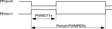
A pulse signal in left aligned mode is generated as follows: At the beginning of the period, the output pin is set to the value in the according bit of the PWMPOL register. The counter PWMCNTx is incremented on each rising clock edge – whatever clock is used as source – and compared to the values in PWMDTYx and PWMPERx. When the counter reaches the value in PWMDTYx, the output pin is inverted, and then is hold on the level until the counter reaches the value in PWMPERx. Here the output pin is set to the original value, and the counter PWMCNTx reset to 0.
|
|
The process for center aligned pulse generation is slightly different: The effective period is twice as long as in left aligned mode. The first half of the period matches the above one. If the counter reaches the PWMPERx value, the pin retains its level, and the counter begins to count backwards. When it passes the PWMDTYx value while it is decremented, now for the second time, the pin changes the level. When the counter gets to 0, again the count direction swaps and a new period begins.
|
|
The 16-bit mode works similar to the 8-bit functionality. As mentioned before, the PWMCNT, PWMDTY and PWMPER registers are grouped into pairs, the even registers (0, 2, 4) act as the high bytes, the odd registers (1, 3, 5) as the low bytes of the 16-bit values. The configuration for polarity, clock selection, alignment, and the output pins is done with the odd numbered bits and pins, as seen in Table 3.3 on page 202.
|
Exactly the same specification exists for an eight channel PWM; the two additional channels are associated to clocks B/SB. The register map increases then 6 bytes in size, and there are no longer unused bits in PWME, PWMPOL, PWMCAE, PWMCLK and PWMCTL.
The model implements the full specification, and turns its attention to performance. This is much more complicated than in the ATD module, because here we have to deal with four different clocks and six completely independent channels. As an example: The PWMCNTx registers contain the current counter value, so the program that runs on the Star12, can determine the progress of a period. A solution to this could be, that an event is generated for each PWM clock cycle, to update the values. But this would lead to excessive event scheduling – possibly every system clock cycle the PWM could produce an event. It is quite obvious that this way may result in poor performance, especially because it is also possible, that no one ever reads the register contents. So the right solution is to start the calculation, when the output signals have to be swapped, and schedule an event for this, and do not care about the counter register. If that is accessed at any time, its value can be calculated dynamically from the system cycle count; the model only has to know when the particular period has started.
The following piece of code shows, how a cycle counter is calculated on demand. The value dTimestamp[x], used to determine when a period has started, is calculated on each period start. See comments for details.
| Listing 3.2: | Checking Routine for PWM |
This may look expensive, but remember this code is only executed, when really a read access to a PWMCNTx register occurs. In line 13 you may notice the comment “already started”, which might be confusing at first sight, because the check whether the channel is enabled, takes place in line 10. But if a channel is enabled, it might be necessary to wait for the clock edge of the particular clock. So the channel may be enabled, though the pulse generation has not started yet. The branch beginning in line 19 shows the extra code necessary for center aligned pulses: The effective period is twice as long as usual, and the counter may run backwards. In most functions there are no discrete branches for 8-bit and 16-bit mode. Period and duty registers are not called directly, but through intermediate values, to ensure transparency for 8-bit and 16-bit concatenated mode of operation. But here, the PWMCNTx registers are actually written, so their values have to be calculated explicitly. In lines 23, 24 and 38 you clearly see that there are the so-called external registers, which are accessed by Octopus, and internal variables having the same values for faster access. This technique also allows a very simple implementation of the double buffering of PWMPERx and PWMDTYx: The Octopus registers are only read, when buffers, pursuant to the specification, are exchanged.
Another difficulty is, that the model should cover two PWM modules. This also is more difficult than in the ATD, because there the additional registers were at the end of the register map, so it is possible to program them statically and then mask the unused part out. Here, the variable part of registers is not at the end of the map, but interleaved. So the module must dynamically create the register map, including the pointers to the access handler functions, which must exist for the biggest possible number of channels, e. g. eight times. Of course these handler functions do nothing more than to invoke a generic handler function for that access type and the type of register.
| Listing 3.3: | PWM generic read check routines |
The function motGetModelData resolves to a pointer to the particular model instance. These callbacks execute the function presented above. To allow dynamic register definition, pointers to these callbacks are collected in an array, so are the register names.
| Listing 3.4: | PWM check callback routines |
Of course the same technique applies for PWMDTYx and PWMPERx registers. The name and function pointers for each register are assembled in a structure, and merged to an array of register structures. This array is then passed to the base class, which will later use the names and callbacks.
A very complicated case was the fact that scaler and prescaler for the clocks can be changed while channels are enabled. Although the specification warns of doing this, because of possible pulse truncations, I had to model the behavior. Additionally there raises the problem of outdated events: If a pulse is generated, an event is always pending. If now the scaler is changed, this event becomes outdated. But Octopus provides no possibility to un-schedule events, so it has to be filtered out when the simulation time reaches that point. The following piece of code shows a part of the Eval callback, where the event filtering is done.
| Listing 3.5: | PWM eval callback |
The remainder of the division offset cycles by cycles per clock shows, if this event was released before a change of scale. It has to be 0 to be current.
Of course, for the PWM, there are the same debugging aids like for the ATD model. If any of the registers PWMPOL, PWMCLK, PWMCAE, PWMPRCLK, PWMSCLA/B are written to, while channels are enabled, a message is generated that warns of possible pulse truncation. There are also warnings for accesses to registers that have no effect or are erroneous, when concatenated mode is active.
Again, there are model manager commands that show the state of the module. Besides registers and ports, the state shows:
A sample output of the Hiwave command line interface looks as in Figure 3.6 on page 208. The model can be configured with respect to the number of channels. It is possible to have 2, 4, 6 or 8 channels. Although the two existing specifications are only for 6 and 8 channels, it was no additional effort to allow also 2 and 4 channels. So the model can be used for four different PWM modules.
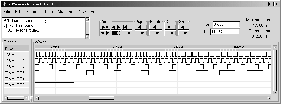
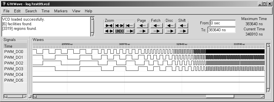
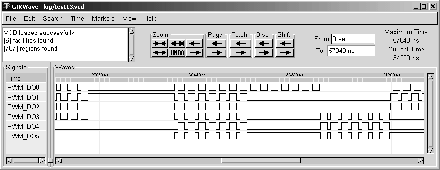
For testing purposes, the VCD dumper, integrated in Octopus, was used. All test cases produce some output. The VCD files then are analyzed graphically, as the expense for rating them automatically would have been too big. As VCD viewer a free tool named GTKwave (see appendix 4 on page 289) was used.
Again the test cases are C programs, compiled and executed automatically. They perform the following test cases, accompanied with some screen shots.
For some test cases, of course, it is necessary to count cycles, but in most cases it becomes immediately obvious if a test case was passed or not.
The PWM module consists of about 1,900 lines of code, additionally about 800 lines of test code.