|
|
Joachim Schlosser: Development and Verification of fast C/C++ Simulation Models for the Star12 Microcontroller
The first module chosen for modeling was the ATD, which is an analog-to-digital converter that provides 10/8-bit resolution and up to 16 analog input channels. For serving the 16 input channels, internal multiplexing is used. The A/D converter has a sample buffer amplifier; the sample time can be programmed. Output values can be left or right justified, signed or unsigned. Several conversions can be pooled in a sequence, whereas a sequence can contain up to 16 conversions, either on one channel or on a series of channels. The start of such a sequence can be triggered externally or by clock, the completion may be signaled with an interrupt. Additionally, the ATD provides the capability to use some or all of the analog input channels as digital input ports ([Sch01]).
|
|
The register map comprises 48 bytes. There are six 8-bit control registers, ATDCTL0 to ATDCTL5. Four are actually used to configure the module, while the two remaining are reserved for future use. The general status register, ATDSTAT0, flags errors and informs about the next target register to be written to. Two other status registers, ATDSTAT2/1, are merged to one 16-bit register and show the sequence progress. A 16-bit test register, ATDTEST0/1, is active in special mode only and contains the values during the approximation process. The 16-bit register ATDDIEN0/1 configures the digital input capability; the values read then appear in PORTAD0/1, with a particular bit being 1 when configured not to act as digital input. The remaining space of the register map is occupied by the 16 data result registers, each 16-bit wide.
There are 21 external pins: Most obvious are the 16 analog input channel pins named PORTAD0-15. Two pins, VDDA and VSSA, act as power source for the analog part of the converter. Another two pins define the lower and upper boundaries for the conversion: VRL and VRH. The last external pin is ETRIG, which is the external trigger input. It may occupy a separate pin or use channel pin 15. For the actual conversion the component owns a “Sample and Hold Submodule”, which includes an analog input multiplexer that selects one of the 16 external analog input channels, the sample buffer amplifier that aids the storage node, and the circuits for the conversion. The resistor and Capacitor DAC arrays produce the comparison values. The comparator uses three stages to compare the input signal to the generated ones. The results are collected in the A/D state machine and the Successive Approximation Register (SAR), a part of the ATDTEST0/1 register.
Concerning the external trigger, there are six different modes of operation defined in section 1.6.2.2 of the specification [Sch01]:
For configuring these modes, four bits in two control registers are used.
Sequences can be configured with respect to the number of conversions they consist of, whether they should work on a single channel or multiple, consecutive channels, and on which channel they are to start. The number of conversions is specified in the SxC bits in ATDCTL3. ATDCTL5 gives the input channel the conversion should be performed or started on with its CD, CC, CB and CA bits . The MULT bit in ATDCTL5 decides, whether to scan a single channel or multiple consecutive channels. Additionally, there is the possibility to specify whether the result registers should or should not map to the conversion sequence, specified with the FIFO bit in ATDCTL3.
The time it takes to perform one conversion depends on different aspects. The conversion clock is a prescaled clock, whereas the prescaler is configured with the 5-bit PRSx value in ATDCTL4, providing a prescaler from 2 to 64 in steps of two. The duration of one of the three sampling phases can be configured with the 2-bit SMPx value in ATDCTL4, making the whole sampling stage either 8, 10, 14 or 22 conversion clock cycles long. The other aspect for timing is the selection of 8-bit or 10-bit conversion, which takes 8, resp. 10 cycles.
This leads to another configure group: the data result configuration. So it is possible to have the results either right or left justified. In left justified mode it is possible to gain signed or unsigned data values. As an example, Table 3.1 on page 180 shows an example for the output codes.
|
The remaining bits of the ATDCTLx registers are used for general configuration, like enabling interrupts, how conversion complete flags are cleared and what has to be done with wait or power down modes.
In test mode, the ATD module can be examined with respect to the power sources and reference pins.
An actual sampling and conversion consists of several phases: First, two cycles are used to sample the signals on the capacitor of the channel. After this, the sample is transferred to the A/D machine’s storage node, which takes another four cycles. Finally the external analog signal is attached directly to the storage node for the configured amount of cycles. This is done to remove possible noise from the signal. After the sampling the conversion takes place, a loop of 8 or 10 cycles, in which consecutively the result bits are generated.
The model is a full implementation of the specification. It includes all configurable operations as well as the test mode. To get a short overview of the interface it presents to Octopus, Table 3.2 on page 183 shows the types of the ports. For modeling analog values, Octopus provides the NUMBER token, which is simply a pointer to a double value. For easier handling, the external trigger input pin is separate, and a digital port.
|
It was a major task to program all the logical connections between the registers and the module’s behavior, as all of the approximately 50 pages of the specification contain information that is linked to other pages. So e. g. if a result register is read from, the corresponding bit in the conversion complete flags register ATDSTAT2/1 has to be cleared, but only if the status register was read before or the AFFC flag was set. Of course, if the debugger generates a backdoor access, the bit must not be cleared to prevent from driving the module in a non-consistent state. The following piece of source code is the handler routine that the base class invokes, if any of the result registers is read from. The main conditional branch checks if the AFFC bit in ATDCTL2 is set. If so, the Conversion Complete Flag associated with the result register that was read can be cleared, although the status register was not read before. Additionally, a possible interrupt can be reset if there are no more unread values. In the other case, an internal variable, indicating the status read, is checked. Here the interrupt reset has not to be performed, because this is done on status reading.
| Listing 3.1: | ATD read routine |
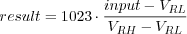
The actual sampling conversion is modeled in a different way to the real hardware, as presented at the end of the previous section. The samples are taken as a single snapshot, not as an average. As there is usually no noise in simulated systems, the process can be omitted to gain simulation performance. The same reason applies to the conversion process, which is performed at the end of the approximation loop. Modeling the conversion process with all details would mean no benefit, as the intermediate values are not used during normal operation. So in the model a conversion takes two stages: The method atd::ConversionTrigger does the sampling at the very beginning of the duration, and calls motNextEvent to evaluate the model 16 to 32 clock cycles later. The Eval callback determines which task is to be performed, and filters outdated events, then executes atd::ConversionExecute, which actually calculates the result. The conversion uses a simple formula, which calculates the proportion of the input value to the range spanned by V RH and V RL, then transforming it into a 10-bit integer, which later can be processed in respect of justification, signed or unsigned, or 8-bit data.
Benefits of using a simulator are not only that no real hardware is needed, but also that a model can aid the software developer with additional information. In the ATD model, i. e. if a write access is performed to a read-only register, like the ATDDRx registers, besides ignoring the access, the user is informed with a warning message. The same applies for all other invalid accesses. If any electrical specification is violated, an error is printed, too.
The ATD module registers several model manager commands to allow the user to get advanced status information. The values of all registers and ports can be printed, in addition to the regular access; and the internal state of the module. The print state command, as an example, shows:
Other information that can be accessed with the commands is a calculation of the current sample rate, as the different control registers define it, and the current electrical specifications of the ATD module. A sample output of the Hiwave command line interface could look like this:
The model is configurable at elaboration time regarding different topics. As the real ATD module can also be implemented with only 8 channels, the model can be configured to act as one of the both kinds of A/D converters. The implementation has e. g. to care about the correct wrap-around when writing to the result registers in FIFO mode. The other topic concerns the electrical specification. Although the specification defines the absolute maximum and minimum values for the analog input ports, the model allows them to be configured. Of course, if no explicit configuration is made, default values are used.
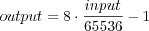
For testing purposes, a second model was developed to produce stimuli for the external input ports of the A/D converter. Though Octopus provides the possibility to use stimuli files for input ports, I decided to use a stimuli model, because the tests can be more dynamic, the test can react on the results the module under test produces. The module is obviously called Digital to Analog Converter (DTA), but does not follow any specification. It is able to produce analog values from -1.0 to +7.0, by writing values from 0x0000 to 0xFFFF to the according registers. One 16-bit register is used for each of the 21 signals. The conversion is performed every time a value is written to any of the registers, it uses the formula:
The test cases are several C programs, compiled and executed automatically; they perform the following test cases:
The test cases can determine on their own whether they passed, it can be seen by the return value, stored in an accumulator. Each bit of the return value stands for another sub test.
Overall, the A/D model consists of about 2,300 lines of code, additionally of about 1,000 lines of test code.
